Conexiant
Login
  • The Analytical Scientist
  • The Cannabis Scientist
  • The Medicine Maker
  • The Ophthalmologist
  • The Pathologist
  • The Traditional Scientist
The Analytical Scientist
  • Explore

    Explore

    • Latest
    • News & Research
    • Trends & Challenges
    • Keynote Interviews
    • Opinion & Personal Narratives
    • Product Profiles
    • App Notes

    Featured Topics

    • Mass Spectrometry
    • Chromatography
    • Spectroscopy

    Issues

    • Latest Issue
    • Archive
  • Topics

    Techniques & Tools

    • Mass Spectrometry
    • Chromatography
    • Spectroscopy
    • Microscopy
    • Sensors
    • Data & AI

    • View All Topics

    Applications & Fields

    • Clinical
    • Environmental
    • Food, Beverage & Agriculture
    • Pharma & Biopharma
    • Omics
    • Forensics
  • People & Profiles

    People & Profiles

    • Power List
    • Voices in the Community
    • Sitting Down With
    • Authors & Contributors
  • Business & Education

    Business & Education

    • Innovation
    • Business & Entrepreneurship
    • Career Pathways
  • Events
    • Live Events
    • Webinars
  • Multimedia
    • Video
Subscribe
Subscribe

False

The Analytical Scientist / Issues / 2013 / Nov / Nano Particle Accelerator
News and Research Technology Materials Science Sensors

Nano Particle Accelerator

Is “accelerator-on-a-chip” technology the tipping point for cheaper, smaller devices for science and medicine?

By Rich Whitworth 11/15/2013 1 min read

Share

Making “lab-on-a-chip” seem a tad pedestrian, researchers at the Stanford Linear Accelerator Center (SLAC) in California, USA, have developed a laser-driven dielectric microstructure – the size of a grain of rice – that can accelerate electrons at ten times the rate of the current SLAC linear accelerator: 300 million electronvolts per meter (1).

1013-202-main.img

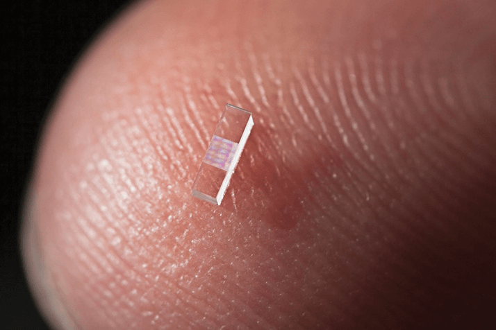
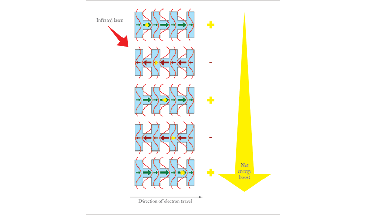
Mind-boggling physics aside, the system is beautifully simple (see Figure 1): near-lightspeed electrons from a conventional accelerator are focused into a 0.5 µm channel within a fused silica glass chip that is patterned with nanoscale ridges. The precisely-spaced ridges cause infrared laser light to generate electric fields that have the net effect of boosting electron energy.

1013-202-fig1Figure 1. How the accelerator-on-a-chip works. The nanoscale pattern increases the laser light’s electric field between the ridges and reduces it within the gaps. Electrons that are perfectly timed with the laser light wave receive a significant net energy gain as they pass through the channel. For video: tas.txp.to/1013-laser

“Our ultimate goal for this structure is one billion electronvolts per meter, and we’re already one-third of the way in our first experiment,” said Stanford professor Robert Byer, the principal investigator for this research, in a SLAC press release. Seeking more economical alternatives to conventional microwave-powered accelerators, Joel England, the SLAC physicist who led the experiments, admitted that there were a number of challenges that must be overcome before the technology is likely to be of benefit to the “outside world”. Primarily, the need for a more compact way of accelerating electrons up to near-lightspeed before they enter the chip must be addressed. Still, with work, the team believe the technology will substantially reduce the size and cost of future high-energy particle colliders, and, said England, “It could also help enable compact accelerators and X-ray devices for security scanning, medical therapy and imaging, and research in biology and materials science.” The term “tabletop accelerator” sounds most tantalizing.

Newsletters

Receive the latest analytical science news, personalities, education, and career development – weekly to your inbox.

Newsletter Signup Image

References

  1. E. A. Peralta et al., “Demonstration of electron acceleration in a laser-driven dielectric microstructure”, Nature, 27 Sept 2013 (10.1038/nature12664).

About the Author(s)

Rich Whitworth

Rich Whitworth completed his studies in medical biochemistry at the University of Leicester, UK, in 1998. To cut a long story short, he escaped to Tokyo to spend five years working for the largest English language publisher in Japan. "Carving out a career in the megalopolis that is Tokyo changed my outlook forever. When seeing life through such a kaleidoscopic lens, it's hard not to get truly caught up in the moment." On returning to the UK, after a few false starts with grey, corporate publishers, Rich was snapped up by Texere Publishing, where he spearheaded the editorial development of The Analytical Scientist. "I feel honored to be part of the close-knit team that forged The Analytical Scientist – we've created a very fresh and forward-thinking publication." Rich is now also Content Director of Texere Publishing, the company behind The Analytical Scientist.

More Articles by Rich Whitworth

False

Advertisement

Recommended

False

False

The Analytical Scientist
Subscribe

About

  • About Us
  • Work at Conexiant Europe
  • Terms and Conditions
  • Privacy Policy
  • Advertise With Us
  • Contact Us

Copyright © 2025 Texere Publishing Limited (trading as Conexiant), with registered number 08113419 whose registered office is at Booths No. 1, Booths Park, Chelford Road, Knutsford, England, WA16 8GS.