
Carbon nanomaterials like graphene, fullerenes, carbon fibers and nanotubes have unique electrical, thermal, chemical and mechanical properties. These properties have inspired significant interest among researchers and innovators who are discovering new applications for graphene in fields such as aerospace, catalysis, photovoltaics, optoelectronics, microelectronics and sensors development.
Raman spectroscopy is ideal for rapid, non-destructive characterization of all sorts of samples, and is well suited for characterizing carbon nanomaterials. In graphene, Raman analysis of several key bands can be used to assess the number of graphene layers and the purity and quality of the sample. The G band observed at ~1580 cm-1 is a good indicator of the number of graphene layers, with band position shifting to lower energy as layer thickness increases, dependent on doping and strain. The G’ band at ~2700 cm-1 can also be used, albeit via a more complex relationship. The intensity of the D band at ~1350 cm-1 is related to the number of defects in the material (amorphous carbon), a marker of purity. It also therefore increases in intensity with the number of graphene layers.
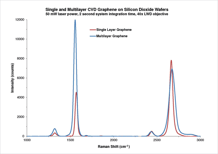
To assess the ability of the Ocean Optics IDRaman microscope with 532 nm Raman excitation to study graphene samples, we measured both single and multilayer samples across the system’s full Raman shift range, 200-3200 cm-1. We used the Clean Peak function in OceanView spectroscopy software to remove background artifacts, capturing high quality data from all three bands of interest. OceanView displays wavenumbers or the Raman shift relative to a specified excitation wavelength. For more sophisticated analysis, a chemometrics software package may be warranted. Although the choice of a short-wavelength 532 nm laser meant autofluorescence generated in the sample could potentially degrade signal to noise and make Raman peaks difficult to resolve, this is not a significant effect for excitation of inorganic materials such as carbon nanotubes and fullerenes.
A shift of ~12 cm-1 was observed for the G band in comparing the single and multilayer samples, while the G’ band width broadened from 39 cm-1 for the single layer sample to 60 cm-1 for the ~4-layer sample (Figure 1). As compared to the 7 cm-1 resolution of the IDRaman micro system, this setup demonstrated performance that is fully capable of building an accurate model of layer thickness. Additionally, the appearance of the D band with an intensity of ~930 counts for the multilayer system demonstrates dynamic range that is more than adequate for assessment of defect levels.
Email: [email protected]
Website: http://oceanoptics.com/application-note-understanding-graphene/
>> Download PDF
Newsletters
Receive the latest analytical science news, personalities, education, and career development – weekly to your inbox.